To design the ATTINY412 echo hello-world board, we used KiCad which is a cross platform and open source electronics design automation suite. I had no expeiences to design schematic, so this week was a bit challenging for me. After installation, you need to set Fab Electronics Library for KiCad to cover all the electronics components found in the official fab inventory. To start, we followed the instructions on this page in gitlab as following:
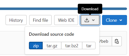
Clone or download this repository. You may rename the directory to fab. For that, go to Download icon near to Clone and download the source code as zip folder (Figure 1). Then, extract the files and store them in a safe place such as ~/kicad/libraries or C:/kicad/libraries.
Figure 1. Downloading the repository
Run KiCad or open a KiCad .pro file.
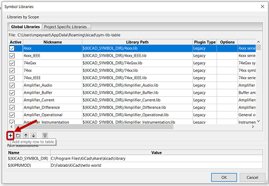
Go to Preferences->Manage Symbol Libraries and add fab.lib as symbol library.
Figure 2. Adding library in KiCad
Go to Preferences->Manage Footprint Libraries and add fab.pretty as footprint library.
Go to Preferences->Configure Paths and add variable named FAB that points to the installation directory of the fab library, such as ~/kicad/libraries/fab or C:/kicad/libraries/fab. This will enable the custom 3D shapes to be found. The 3D shapes project has just started and most of them have to be populated still.
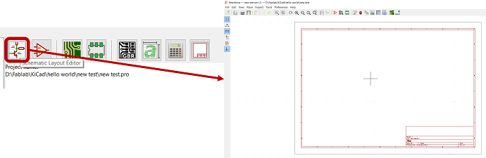
Create a new project in KiCad and open Schematic Layout Editor which will guide you to Eeschema page. (Figure 3)
Figure 3. Opening Schematic Layout Editor in KiCad
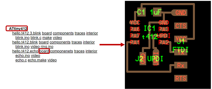
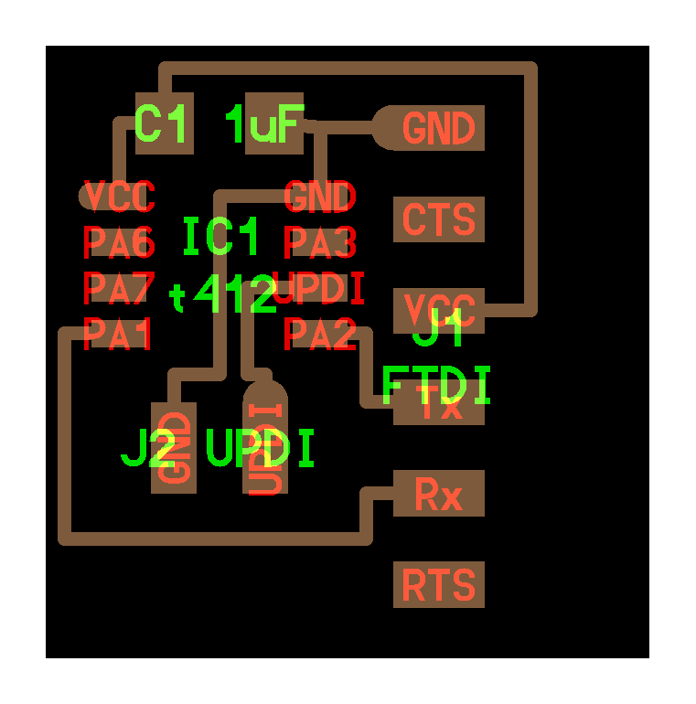
Figure 4. The ereference image of the ATtiny412 board
The list of the components we used is as the following:
Conn_FTDI_01x06_Male
CAP_UNPOLARIZEDFAB
Conn_01x03_Male
GND
VCC
LEDFAB1206
BUTTON_B3SN
Microcontroller_ATtiny412_SSFR
R1206FAB(1KΩ)
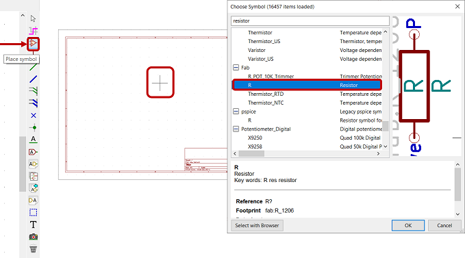
From the toolbar on the right side, choose Place symbol. Next, simply click on the place you want to put the symbol and then, the list of symbols will be appreared. After typing the symbol, you should choose it from the fab library.
Figure 5. Placing and choosing symbols in KiCad
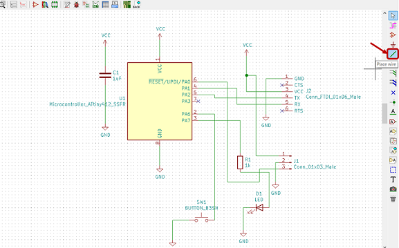
After placing all the symbols, you should connect them with wire (Go to Toolbar and choose Place wire). Be careful while connecting the components, not to cross other paths to prevent short circuits.
Figure 6. Placing wire and the final schematic design
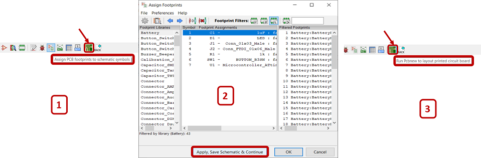
Then, go to Assign PCB footprints o schematic symbols and apply it. Next, go to Run Pcbnew to layout printed circuit board.
Figure 7. Adding footprints and Run Pcbnew in KiCad
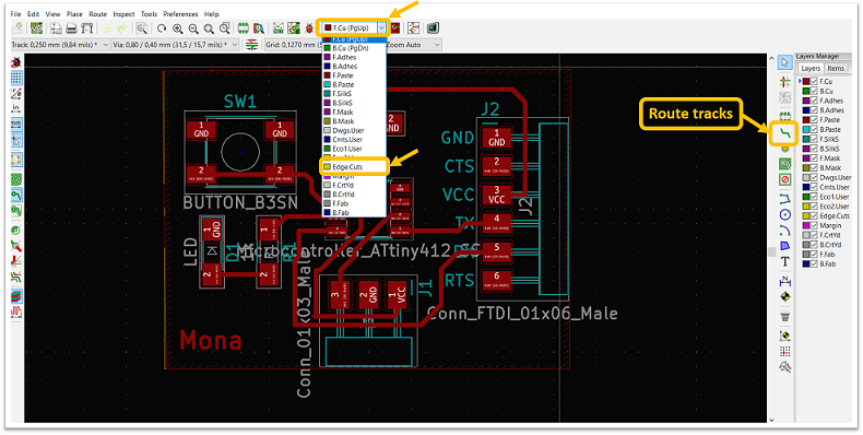
Then, on Pcbnew page, first, you should check the layer to be front Copper from the top toolbar that is set to F.Cu (PgUp) (For edges, it should be set as Edge.Cuts). Next, go to Route tracks on the right toolbar and try to connect the drawn tracks in a way not to cross each other. This might be tricky!
Figure 8. Route tracks in KiCad
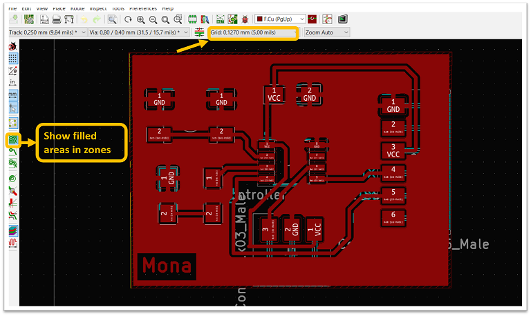
To display the filled areas, just click on the icon showed in Figure 8 from the left toolbar and to remove it, click on the icon below it. Also, you can change the grid setting by adjusting the mills from the top toolbar.
Figure 9. Show filled areas in zones in KiCad
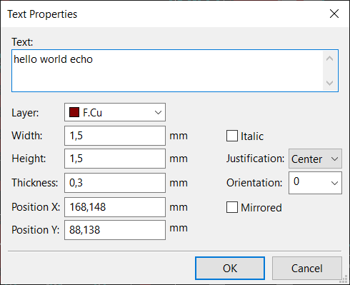
You can also add text to your board by going to Plcae->Text and click on your desired place for the text.
Figure 10. Adding text in KiCad
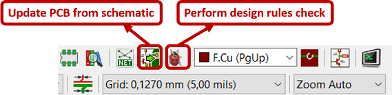
Then, update PCB from schematic and also, perform design rules check as it is shown in Figure 11. At this stage, I faced some errors originated from differences in naming librarires and symbols were chosen from their list that I solved it with the help of our local instructor and my groupmates.
Figure 11. Updating PCB from schematic in KiCad
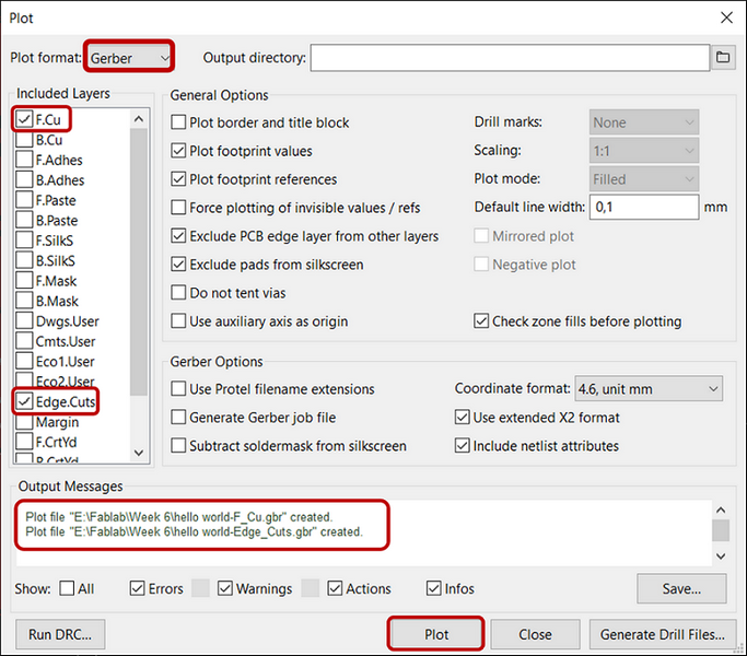
Now, the board is ready for milling. But for LPKF milling machine, we need Gerber (.gbr) format of the file. Go to File->Plot and select F.Cu and Edge.Cuts from the layers and then, click Plot which will automatically, generate .gbr files.
Figure 12. Generating .gbr files in KiCad
Milling with LPKF
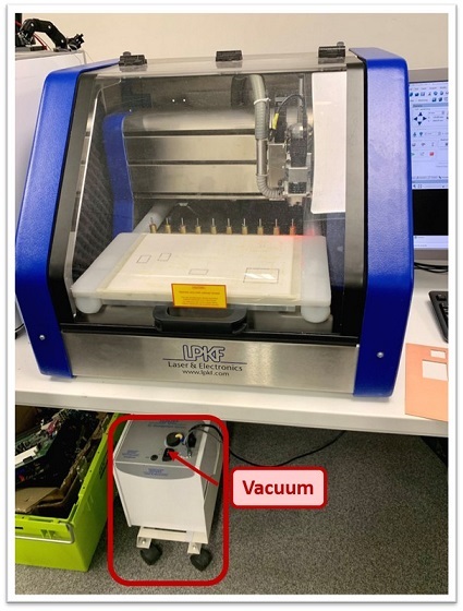
For milling, we had a newly-arrived milling machine in Fablab Oulu called LPKF ProtoMat® S62which has many advantages compared to Rolland milling machine including:
Superior milling speed, resolution and accuracy
Automatic tool change for unmatched ease-of-use
Vacuum table and fiducial recognition available
Figure 13. LPKF ProtoMat® S62
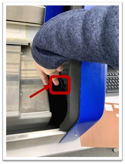
Open the chamber and turn on the machine through the button on the right corner (Figure 13).
Figure 14. Switch on the machine
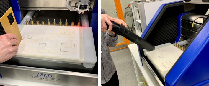
Before putting the blank PCB (Copper-clad laminate (CCL)), you should ensure that the table is completely clean and with no dust. So, you can use another blank PCB or air vacuum.
Figure 15. Cleaning the surface of the table with a blank PCB and air vacuum
Then, put the blank PCB and fix it all around with a tape.
Figure 16. Fixing the blank PCB on the table in LPKF
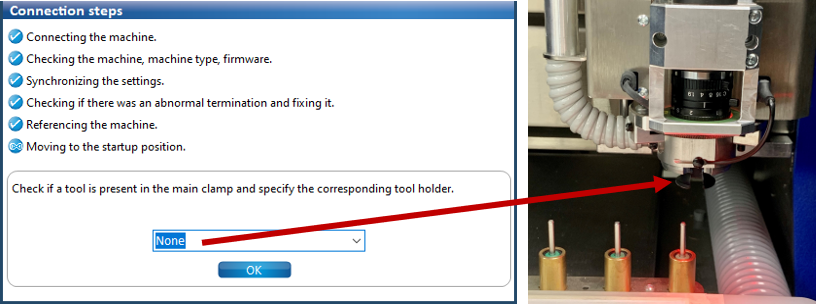
First, launch the software of the machine which is LPKF CircuitPro PM 2.7. Then, this window will appear on the screen showing the connection steps and check if none of the tools is in the main clap. Click OK.
Figure 17. The connection steps checking
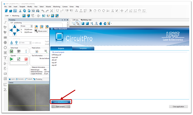
Then, open a new document and select Load default template.
Figure 18. Open a new document in CircuitPro PM 2.7
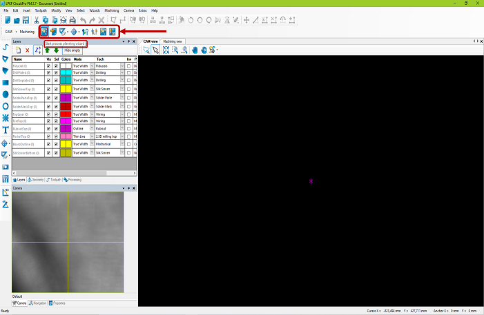
Now, go to the toolbax for Machining and start to set them one by one from the left. First, go to Start process planning wizard.
Figure 19. Start process planning wizard in CircuitPro PM 2.7
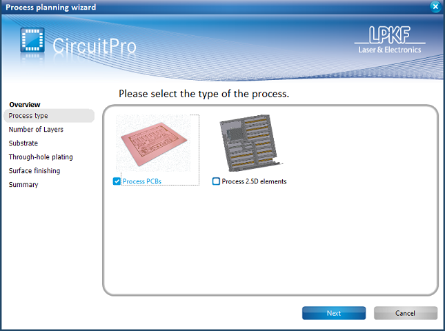
Choose Process PCBs and click Next.
Figure 20. Selecting the type of process in CircuitPro PM 2.7
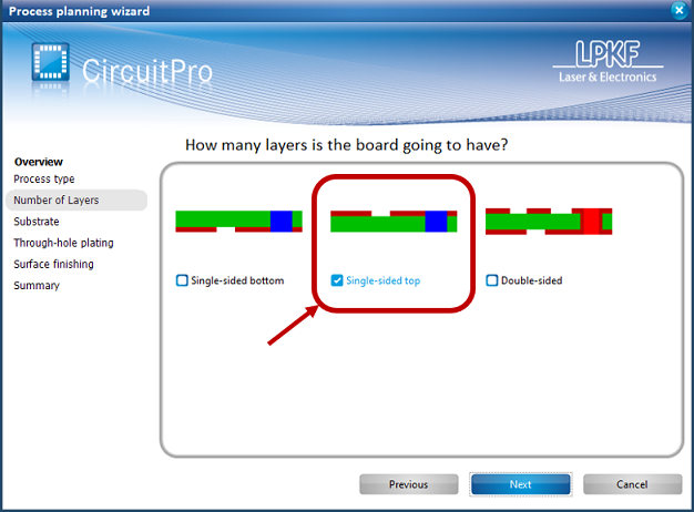
Next, define the number of layers which for our case would be Single-sided top.
Figure 21. Selecting the number of layers in CircuitPro PM 2.7
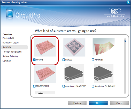
Then, select the kind of substrate which would be FR4/FR5.To have a clue of the differences of Fr1-FR4 materials, you can have a look here.
Figure 22. Selecting the kind of substrate in CircuitPro PM 2.7
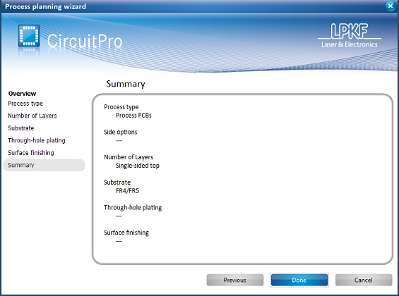
Next, jump to Summary and double check the process planning and click Done.
Figure 23. Summary of the process planning in CircuitPro PM 2.7
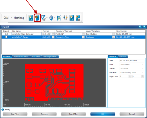
Then, import the files you have saved from KiCad in .gbr format.
Figure 24. Importing the .gbr file generated in KiCad to CircuitPro PM 2.7
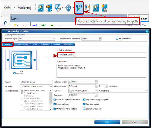
Next, jump to Generate isolation and contour routing toolpath and from Isolate, set the isolation method as Complete rubout
Figure 25. Selecting the isolation method in CircuitPro PM 2.7
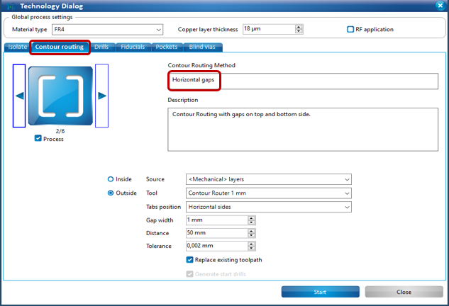
From Contour routing, set the contour routing method as Horizontal gaps
Figure 26. Selecting the contour routing method in CircuitPro PM 2.7
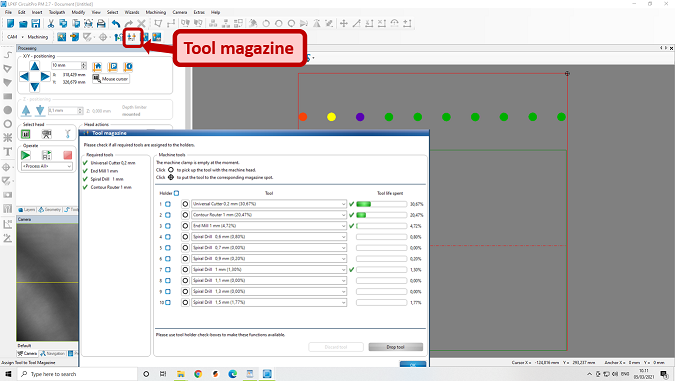
Next, you can check the machine tools life spent in Tool magazine.
Figure 27. LPKF tool magazine
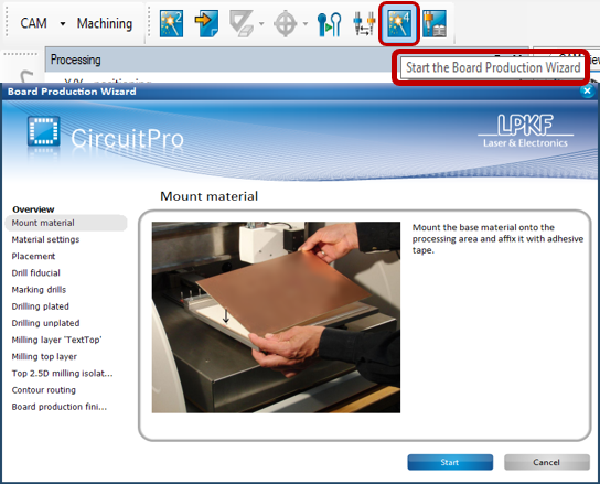
Go to Start the Board Production Wizard and click Start.
Figure 28. Start the Board Production in CircuitPro PM 2.7
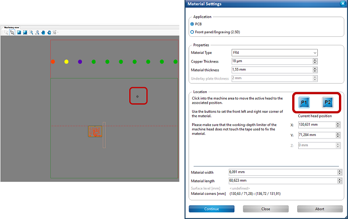
Then, material settings opens up where you should define where to place the board in the milling area and P1 (left lower corner) and P2 (right upper corner). But remember clicking on P1 and P2 buttons should be done after setting the corner points. For now, just put the mouse pointer somewhere in the work area.
Figure 29. Setting the place of the board in the milling area
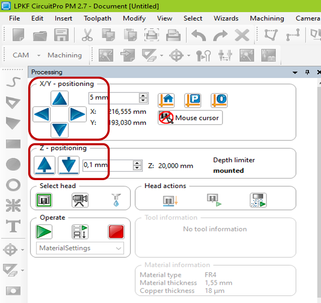
First start from setting P1 (lower left) and simply navigate the tool head on the optimized position through X/Y and Z positioning. When you find the desired position, you can press P1. The same process will be used for P2 but for the top right area. You can define an area bigger than the size of your board. After setting the location of the milling area, press Continue.
Figure 30. Navigating tools in CircuitPro PM 2.7
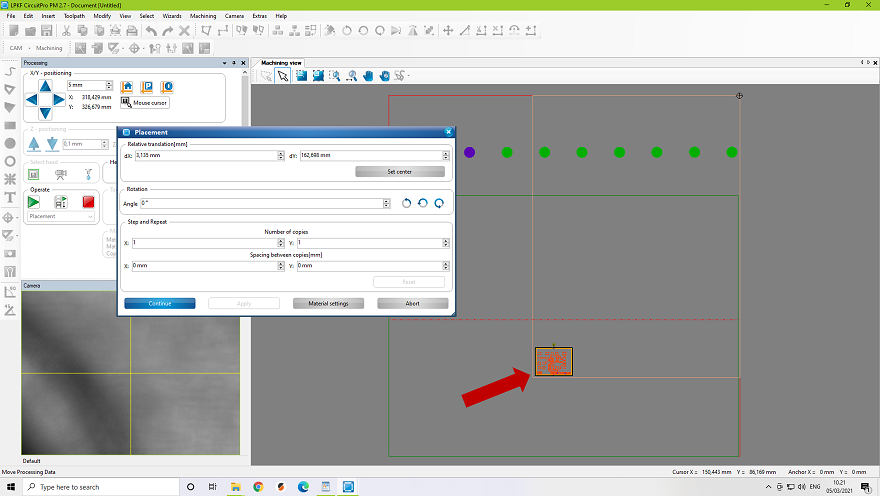
After clicicking Continue in Material Settings, the head of the machine will be moved to the defined place. When Placement opens up, move the board to the defined milling area (better to be close to the corber to avoid waste of material).
Figure 31. Moving the board to the defined milling area
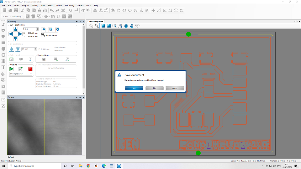
Next, click Continue and after that, you can save the changes in settings for further applications.
Figure 32. Saving the changes in Settings
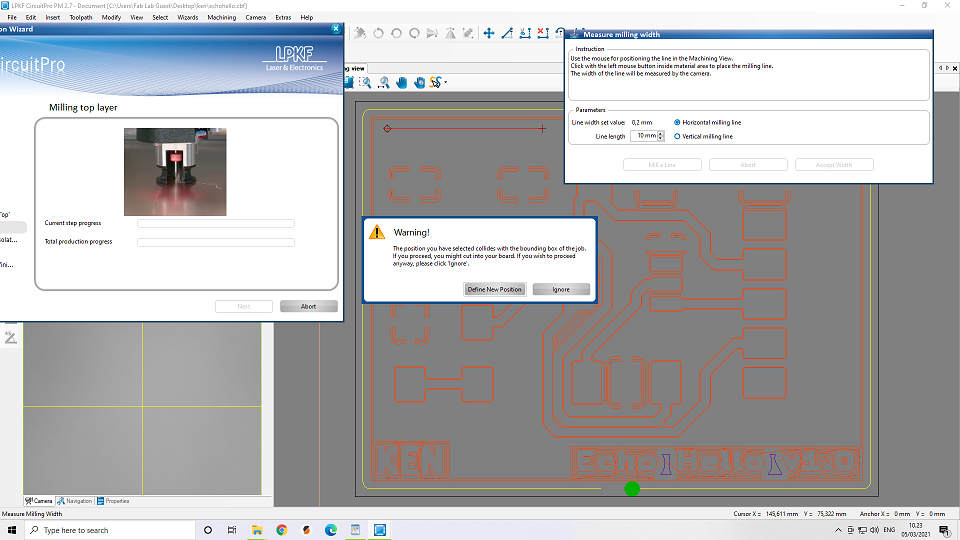
Then, it can start the processing with measuring milling width. But we faced a warning that the selected position have collieds with the bounding box of the job although we ignored it.
Figure 33. Warning before measuring milling width
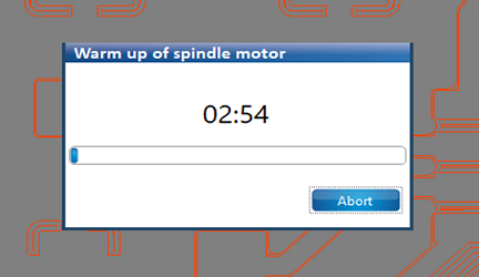
Wait for the spindle motor warming up. It might take a couple of minutes
Figure 32. Warm up of spindle motor in CircuitPro PM 2.7
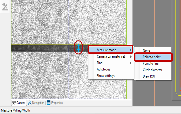
Now you should calibrate the focus height of the camera. Go to the Camera view and right-click; go to Meausure mode->Point to point and set the line arrow.
Figure 33. Measure mode in camera view in CircuitPro PM 2.7
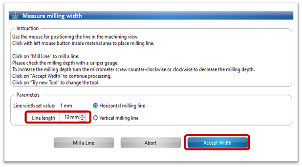
Finally, set the Line length as 10 mm and Accept Width.
Figure 34. Accepting width of the line length in CircuitPro PM 2.7
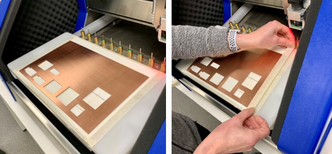
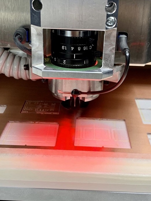
When milling is finished, again apply air vacuum or a wet cloth to clean the PBC surface.
Figure 35. Milling PCB in LPKF
Software for LPKF
Milling the board with LPKF
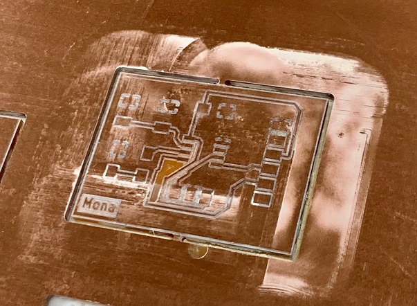
Figure 35. Milled PCB appearance in LPKF
Now, simply twist the board from the vertical axis to unattach your board from the blank PCB.
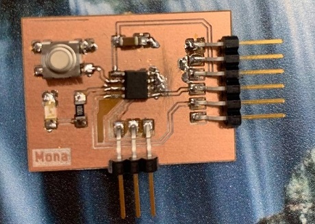
Now, it's soldering time! Pick the components you need and solder them on the right position based on the reference board.
Figure 36. Final soldered board
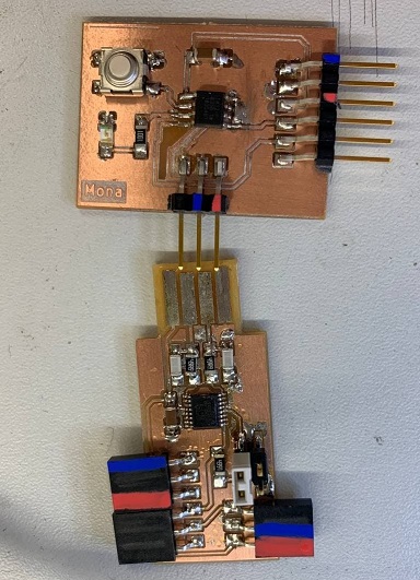
With the suggestion of my groupmate, Antti, I tried to recognize the gorund and VCC connections for both boards and mark them with colorful markers.
Figure 37. Marking the ground and VCC on the boards
Testing the board
For testing the board, I used the UPDI programmer made during Week 4 (Electronics Production). Then, I attached it to the new board and a USB cable and connected it to my computer.
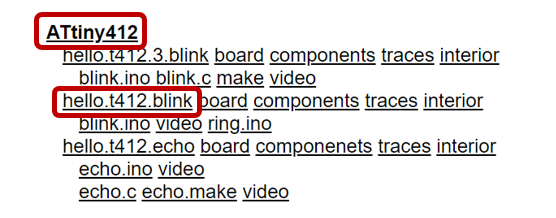
Then, open Arduino and from Embedded Programming page, go to ATtiny412->hello.t412.blink and copy-paste in a new sketch in Arduino and click Upload.
Figure 38. Finding the sketch file from Embedded Programming page
If everthing goes well and no error apears, you will face this amazing scene after all your efforts!:)
This week, I had a totally new experience in designing schematic with KiCad and also, milling with a new milling machine (LPKF). So, it was a bit challenging in the beginnig, but with the help of our great local instructor, Antti, and my groupmates, I could pass the obstacles. For soldering, I had a bit experience from the Week 4 and I was more confident although still keeping be cautious! In general, I really enjoyed designing in KiCad and I am sure in the coming weeks, I will get more experience and skills.
